
The structural design of the component layout and electrical connection of a high-performance PCB is a key factor in determining whether the electrical control equipment can work reliably. For circuits with the same components and parameters, different component layout designs and electrical connection methods will produce different results, and the results may be very different. Therefore, it is necessary to consider how to correctly design the structure of the PCB component layout and correctly select the wiring direction and the process structure of the overall equipment. A reasonable process structure can not only eliminate the noise interference caused by improper wiring but also facilitate installation, debugging, and maintenance in production. In order to maximize production and minimize costs, certain restrictions should be taken into account.
1. Structure of PCB component layout
The welding technology and equipment required for PCB assembly add many limitations to the design and layout of the circuit board. For example, in wave soldering, the maximum size of the groove, the distance between the edges, and the space for operation are all important factors. At the same time, the designer should be as aware as possible of what the final product should look like and try to protect its most sensitive parts. For example, any high-voltage circuit should be protected from contact with the outside; the circuit boards in the product and the components on the circuit boards should be carefully placed to minimize damage caused by external objects.
2. Correctly select the wiring direction
Due to the existence of extremely small noise voltages generated by the wiring of the PCB amplifier, the output signal will be severely distorted. Therefore, the wiring direction must be correctly selected. In digital circuits, the TTL noise tolerance is 0.4~0.6V, and the CMOS noise tolerance is 0.3~0.45 times of Vcc, so digital circuits have strong anti-interference capabilities.
Reasonable selection of good power and ground bus methods is an important guarantee for reliable operation of equipmtent, because quite a lot of interference sources are generated through the power and ground buses, among which the noise interference caused by the ground wire is the largest.

3. The process structure of the overall electrical control equipment
The assembly method of multiple circuit boards usually makes on-site maintenance as easy as pulling out the circuit board for replacement. Of course, the prerequisite is that each independent circuit board can perform its unique function, so that the replacement of the circuit board will not involve too much disassembly, ensuring the minimum number of soldering/desoldering times. Therefore, the design of the PCB must take its maintainability into consideration.
4. The influence of the processing technology level of the PCB
(I) If the wire spacing is less than 0.1mm, the etching process cannot be carried out, because if the etching liquid cannot effectively diffuse in the narrow space, part of the metal will not be etched away.
(2) If the wire width is less than 0.1mm, it will break and be damaged during the etching process.
(3) The pad size should be at least 0.6mm larger than the hole size.
(4) The minimum or maximum circuit board operating size.
(5) The accuracy of the etching equipment.
(6) The drilling accuracy.
5. The influence of the PCB plate making method
(I) Determined by the camera size performance of the original film of the product.
(2) The accuracy that can be achieved by the screen printing process.
6. The influence of the PCB assembly
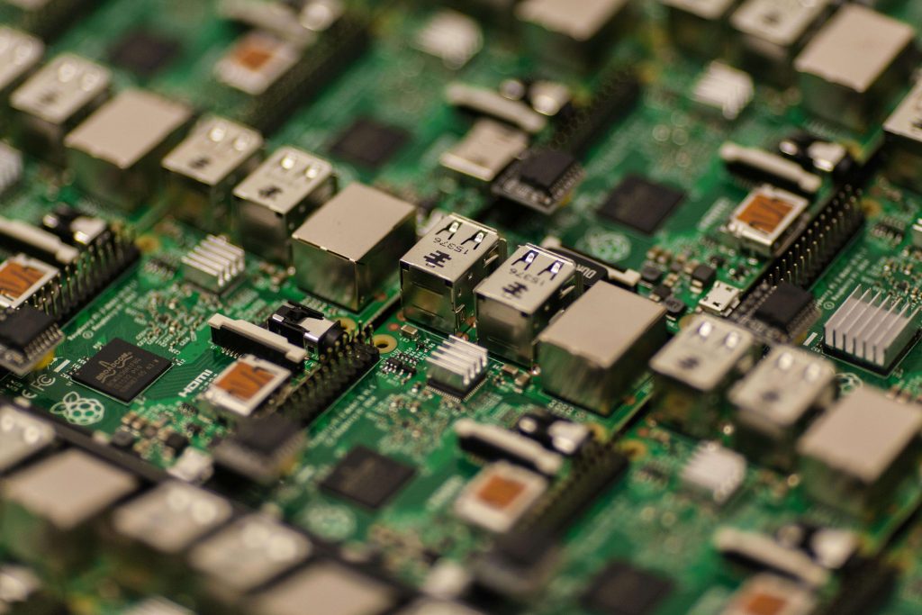
(I) The diameter of the hole should be determined based on the maximum material condition (MMC) and the minimum material condition (LMC). The diameter of an unsupported component hole should be chosen such that the MMC of the pin is subtracted from the MMC of the hole, leaving a difference between 0.15 and 0.5 mm. Furthermore, for strip pins, the difference between the nominal diagonal of the pin and the inner diameter of the unsupported hole should not exceed 0.5 mm and should not be less than 0.15 mm.
(2) Smaller components should be placed so that they are not obscured by larger components.
(3) The thickness of the solder resist should not exceed 0.05 mm.
(4) Silkscreen markings should not intersect any pads.
(5) The top half of the board should be the same as the bottom half to achieve structural symmetry, as an asymmetrical board may bend.
From the perspective of board assembly, special attention should be paid to the short circuit problem that may be caused by the tilt of the inserted component relative to its theoretical position before soldering. As a rule of thumb, the maximum allowable tilt of the component pins should be kept within 15° of the theoretical position. When the difference between the hole and the pin diameter is large, the tilt can be up to 20°. For vertically mounted components, the tilt can be 25° or 30°, but this will result in a reduction in packaging density. For example, if the TO-I8 transistor is mounted 2mm from the thickness of the PCB, if the hole diameter is 1mm, the tilt can be 20°, of course, the pin itself has no tilt.