
1. PCB Design
PCB design begins with determining the board’s dimensions, constrained by the enclosure or mounting space. The board must fit within the housing. Designers must also plan for connections between the PCB and external components, such as potentiometers or sockets, using plastic or metal wires. Occasionally, socket designs are used, allowing easy insertion into a connector.
Large components on the PCB should be secured with metal brackets to enhance resistance to vibration and impact.
2. Layout Design Techniques
First, thoroughly understand the specifications, sizes, and dimensions of components and sockets. Plan their positions carefully, focusing on electromagnetic compatibility and minimizing interference. Ensure shorter and fewer intersecting traces. Proper arrangement of power, ground paths, and decoupling is essential.
Once component positions are finalized, connect their terminals according to the circuit diagram. Both manual and computer-aided design (CAD) methods can be used.
- Manual Layout: Time-consuming but useful for beginners.
- CAD Tools: Efficient for editing, storing, and printing designs.
After determining PCB dimensions, roughly position components and refine the layout iteratively for optimal efficiency.
3. Component Wiring Guidelines
- Avoid crossing traces. Solve crossovers by routing through gaps or looping around other traces. Complex circuits may use jumpers or double-sided boards.
- Components like resistors and capacitors can be mounted vertically or horizontally, affecting space usage and mechanical strength.
- Place same-circuit ground points close together. Attach power filter capacitors near these points to avoid interference.
- Arrange main ground lines in high-to-low frequency order, avoiding random connections. This is crucial for devices like frequency converters. Use large ground planes for shielding high-frequency circuits.
- Use wider traces for high-current lines to reduce resistance and minimize parasitic coupling.
- Keep high-impedance traces short to avoid instability. Low-impedance traces, such as power and ground, can be longer. Separate audio channels until the power amplifier stage to prevent crosstalk.
4.Basic Rules for Layout of Electronic Components on Printed Circuit Boards (PCB)
The layout and routing of components on a PCB significantly influence product lifespan, stability, and electromagnetic compatibility. To ensure a high-quality, cost-effective PCB design with optimal electronic performance and interference resistance, the following principles must be observed:
1. Layout Plan Determination
- Define the board’s dimensions based on the structural diagram, placing mounting holes and connectors. Lock these components and annotate dimensions per design standards.
- PCB size selection is critical. Larger sizes increase trace length, resistance, noise susceptibility, and cost; smaller sizes compromise heat dissipation and increase interference risk. Rectangular boards with aspect ratios of 3:2 or 4:3 are ideal. For boards exceeding 200mm x 150mm, mechanical strength must be considered.
- Allocate no-layout zones based on component requirements and manufacturing constraints. Reserve space for mounting holes and supports.
- Optimize PCB performance and manufacturing efficiency through the appropriate processing flow.
2. Basic Layout Principles
- Follow the “big-to-small, complex-to-simple” placement rule. Prioritize essential circuit units and key components.
- Group related circuits into modules. Maintain proximity within modules while separating analog and digital circuits.
- Arrange key components according to signal flow, ensuring minimal critical signal trace lengths and proper signal separation (e.g., high-current vs. low-current, analog vs. digital).
- Use symmetric layouts for similar circuit sections to simplify design and testing.
- Optimize component placement for uniform distribution, balance, and aesthetic considerations.
- Adhere to grid settings, such as 50-100mil for ICs and 25mil minimum for small surface-mounted devices.
3. Component Placement Sequence
- First, position structural components like power connectors, LEDs, and switches. Lock their locations to avoid unintentional shifts.
- Place specialized or large components (e.g., transformers, ICs) before arranging smaller components.
- Arrange components logically according to the circuit’s signal flow to streamline connectivity.
- Center layouts around critical components, minimizing interconnections to improve reliability and performance.
4. Dimension and Placement Requirements
- Resistors: Flat-mounted resistors use 4/10 inch spacing for ¼W, 5/10 inch for ½W. Adjust spacing for vertical arrangements in compact designs.
- Proximity: Keep components at least 2mm from PCB edges and avoid placing components within 1.27mm of non-mounting holes.
- Spacing: Ensure a minimum distance of 2mm between metal components and traces. Follow specific spacing rules for wave-soldered and press-fit components.
- Clearances: Maintain a 5mm gap around BGA components and similar spacing for adjacent surface-mounted components.

5.Placement and Direction Requirements
- Power Sockets:
Power sockets should be arranged around the edges of the PCB. They should be placed on the same side as their connecting bus terminals. Avoid positioning power sockets or solder connectors between other connectors to facilitate welding and cable management. Ensure adequate spacing for plugging and unplugging power connectors. - Adjustable Components:
Layout adjustable parts like potentiometers, variable inductors, and capacitors per structural needs. Internal adjustments should be easily accessible on the PCB. External adjustments must align with panel controls. Potentiometers should increase output voltage when turned clockwise. Place potentiometers near the edges with handles facing outward. - IC Sockets:
Ensure IC socket alignment by verifying the positioning notch orientation. Pin 1 must be at the lower right or upper left near the notch. Align ICs and clearly indicate polarities, limiting them to two perpendicular directions on a PCB. - Directional Consistency:
Similar components should align consistently in the X or Y direction. Polarized components should follow the same polarity markings for ease of production and inspection. - Debugging and Maintenance:
Arrange components for easy debugging and repair. Avoid placing large components near smaller ones. Ensure sufficient space around adjustable components. - Decoupling Capacitors:
Position decoupling capacitors near IC power pins, minimizing loop lengths between power and ground. - Power Grouping:
Group devices sharing the same power supply to simplify power segregation. - SMD Components:
Align SMD components on one side, ensuring consistent character orientation and packaging direction.
6.Heat Dissipation Considerations
- Heat Distribution:
Distribute high-power components like power transistors and transformers along edges to dissipate heat. Avoid concentrating heat sources in one area. - Proximity to Capacitors:
Keep heat-generating components away from electrolytic capacitors to prevent premature aging. - Sensitive Components:
Distance heat-sensitive components and wiring from high-temperature devices. - Temperature Sensors:
Place sensors for tempe rature detection near heat sources but away from sensitive components.
7.Additional Layout Requirements
- Via Placement:
Avoid vias under horizontal resistors, inductors, and capacitors to prevent short circuits during wave soldering. - Copper Filling:
Ensure balanced PCB wiring density, filling sparse areas with mesh copper foil with grid lengths over 8 mils. - Solder Pads:
Do not place vias on SMD solder pads to prevent solder paste leakage and false connections. Avoid routing critical signal traces between socket pins. - Wave Soldering:
Use non-plated holes for fastening and positioning on wave-soldered boards. Ground mounting holes through distributed grounding vias. - Impedance Matching:
Place matching resistors and capacitors near signal sources or terminals. Limit resistor distance to 500 mils from drivers. - High-Frequency Connections:
Minimize high-frequency wiring lengths and prevent electromagnetic interference. Keep inputs and outputs far apart. - Component Proximity:
Maintain adequate spacing between high-potential parts to avoid arcing or short circuits. Place high-voltage components in areas difficult to touch during testing. - Heavy Components:
Secure components over 15g with brackets before soldering. Install large, heat-generating parts on the chassis for better heat dissipation.
4.PCB Component Routing Rules
Post-Layout Verification
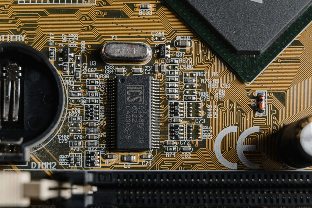
After completing the layout, print the assembly and schematic diagrams. The designer must verify component packaging accuracy and confirm signal correspondence among boards, backplanes, and connectors. Routing may begin only after confirmation.
1) Routing Principles
- Routing Direction:
From the soldering side, component arrangements should align with the schematic. Keep routing direction consistent with circuit diagrams to facilitate inspection, debugging, and maintenance. - Terminal Arrangements:
- Minimize distance between related terminals (preferably 0.2–0.3 inches).
- Group input/output terminals on 1–2 edges for clarity.
- Lead Arrangement:
Design pin arrangements logically and maintain appropriate spacing between component pins. - Routing Rationality:
Ensure straightforward and ordered routing while meeting circuit performance requirements. Minimize vias and jumpers to improve production, debugging, and maintenance convenience. - Routing Surface:
Prefer routing on the soldering side, especially for through-hole PCBs. - Copper Foil Usage:
Avoid large copper foil areas as they may delaminate under prolonged heat. Use grid patterns to release volatile gases. - Minimized Bends:
Reduce routing bends for clarity. Avoid sudden width changes or sharp turns. Maintain corners above 90°.
2) Dimension Requirements
- Restricted Areas:
Do not route within 1mm of PCB edges or mounting holes. - Minimum Widths:
- Power lines: ≥18 mil.
- Signal lines: ≥12 mil.
- CPU I/O lines: ≥10 mil.
- Via Sizes:
- Standard vias: ≥30 mil diameter.
- Pad Sizes:
- Dual-inline pads: 60 mil (pad), 40 mil (hole).
- 0.25W resistors: 51×55 mil for SMD; 62 mil (pad), 42 mil (hole) for through-hole.
- Non-polar capacitors: Same as above for corresponding mounting methods.
- Critical Lines:
Zero-voltage and power lines should be ≥1mm wide.
3) Trace Width and Spacing
- Minimum Widths:
The trace width depends on current flow and adhesion to the substrate. For 2A current and 0.05mm copper, a 1.5mm trace suffices. - Spacing Considerations:
Spacing between traces depends on insulation resistance and breakdown voltage. For digital circuits, allow 5–8 mil if the process permits. - High-Voltage Isolation:
Separate high-voltage and low-voltage lines based on voltage endurance. For example:
- 2kV requires a 2mm distance.
- 3kV requires ≥3.5mm.
To prevent arcing, add slots between high and low voltage areas.
- Current and Voltage Signals:
Isolate high-current and high-voltage signals from small signals to reduce interference.
4) Pads
- The pad diameter must be slightly larger than the lead diameter. Pads that are too large may cause weak soldering. The outer pad diameter D should typically be at least (d+1.2mm), where d is the lead hole diameter. For high-density digital circuits, a minimum diameter of (d+1.0mm) is acceptable.
- Pads on single-sided boards must be larger, and connected traces must be thicker.
- Pad spacing should align with the lead spacing of the corresponding electronic component.
5) Anti-Interference Requirements
Power Line Design
- Increase the width of power lines based on the current to reduce loop resistance. Ensure power and ground lines follow data transmission directions to enhance noise immunity.
- Position power and ground lines close together and distribute them in a grid-like structure to balance currents.
Ground Line Design
- Separate digital and analog grounds. Logic and linear circuits should remain distinct. Use single-point connections for low-frequency circuits. For high-frequency circuits, adopt multi-point connections with short and wide ground lines.
- Thicker ground lines reduce voltage variation and improve noise immunity. Ideally, ground line width should accommodate three times the maximum current and measure 2–3 mm.
- Create a closed-loop ground circuit for digital-only boards to improve noise resistance.
Decoupling Capacitors
- Add RC decoupling at control line inputs to eliminate interference.
- Use 10–100 µF electrolytic capacitors at power inputs, or higher if possible.
- Place a 0.01 µF ceramic capacitor near each IC chip. If space is limited, use one capacitor for every 4–8 chips.
- Install decoupling capacitors between power and ground lines of noise-sensitive components like RAM and ROM.
- Keep capacitor leads short, especially for high-frequency bypass capacitors.
- Use R-C circuits to absorb discharge currents in components like relays and switches. Typical values are R=1–2kΩ,C=2.2–47μF.
- Use decoupling capacitors between power and ground for logic circuits. Avoid high-speed logic if unnecessary.
CMOS Devices
Unconnected CMOS inputs must connect to ground or a positive power supply to prevent interference.
Dual-Sided Routing
- Orient traces on opposite sides orthogonally to reduce parasitic coupling.
- Input and output lines should avoid parallel routing. Place a ground line between them to minimize feedback.
Additional Guidelines
- Use radial layouts for power and ground lines, avoiding looped routing in signal lines.
- Increase spacing between traces or insert zero-volt lines for isolation when necessary.
- Reserve dedicated zero-volt lines for analog circuits.
6) Other Routing Considerations
- For high-frequency circuits, keep traces short and thin. Use curved corners instead of sharp angles.
- Maintain similar lengths for address and data lines. Adjust shorter lines with compensatory bends.
- Copper Pouring:
- After routing, fill unused areas with copper, preferably grounded. Avoid connecting to VCC\text{VCC}VCC unless required to handle high current.
- Use grid patterns to prevent bubbling or warping during soldering. Ensure complete grounding for copper pours.
- Signal Shielding:
- Use “guard ground” by enclosing critical signal lines with two ground lines to reduce interference.