
1. Definition of Terms
- Horizontal Components: Components where the line connecting the two leads is parallel to the line connecting the reference and auxiliary positioning holes.
- Vertical Components: Components where the line connecting the two leads is perpendicular to the line connecting the reference and auxiliary positioning holes.
2. Auto-Insertion PCB Drawing Requirements
Follow all specifications and design rules as described below to ensure compatibility with auto-insertion machines.
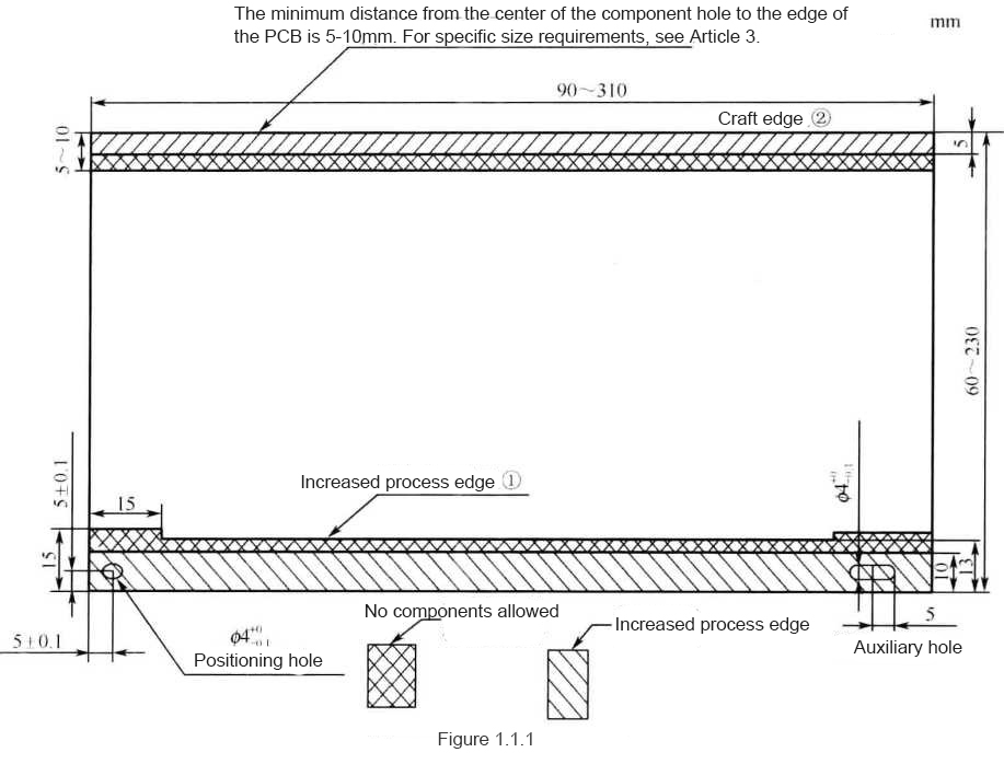
3. Auto-Insertion PCB Design Standards
1) PCB Dimensions
- Auto-insertion machines support PCB sizes from 90 × 60 mm to 310 × 230 mm.
- PCBs may be combined into panels when necessary, or left as individual boards.
2) Positioning Holes
- Reference Holes: Circular, 4 mm diameter.
- Auxiliary Holes: Oval, 4 × 5 mm dimensions.
- Distance from the center of any hole to the PCB’s edge must be 5 mm.
- The centerline connecting reference and auxiliary holes must maintain a parallelism tolerance of ±0.1 mm to the PCB edge.
3) Process Edge
- Use process edges only if required. Ensure they do not interrupt traces or silkscreen elements.
- Maintain a minimum 5–10 mm distance from auto-insertion component holes to PCB edges. Add a 3–5 mm process edge if necessary.
- Shaded areas in design (refer to diagram) must remain free of auto-insertion components.
4) Positioning Holes on Process Edges
- To save material, positioning holes may be placed on process edges. For smaller process edges, increase perforation points to prevent detachment during handling.
5) Adjusting Process Edges
- Ensure a rectangular or square PCB shape. Corners or middle edges may include cutouts or additional process edges.
6) Component Count
- A single PCB must have at least 80 auto-insertion components. Alternatively, production analysis can determine if a PCB requires auto-insertion design.
7) Placement of Positioning Holes
- Place holes on the side with fewer components.
- Avoid interrupting traces or conflicting with other positioning requirements.
- Every board should ideally include positioning holes for compatibility.
8) Component Placement
- Auto-insertion components must not be placed in shaded areas of the design. Non-auto-insertion components are permitted but must comply with soldering clearance requirements.
- Maintain proper spacing for horizontal and vertical components to ensure alignment and solderability.
9) Standard Component Library
- Use components with predefined specifications:
- Horizontal components: Resistors, jumpers, diodes, etc., with 10 mm lead spacing.
- Vertical components: Capacitors, transistors, etc., with 5 mm lead spacing.
10) Identification Markings
- Place identification markings in non-interfering locations. Use a 3 mm diameter circle with a 1.5 mm center dot, accompanied by numeric identifiers.
4. Manufacturer Requirements
- Tolerance for component hole center distances is ±0.05 mm (reduced to ±0.03 mm on-site).
- Component holes must feature a flared design to accommodate insertion.