
1. Considerations in Design
When determining the shape, pad patterns, and wiring methods of surface-mount PCB, consider assembly type, mounting method, placement precision, and soldering processes. This ensures high soldering quality and enhances module reliability. SMT (Surface Mount Technology) and THT (Through-Hole Technology) PCB design standards differ significantly.
Designers should not only understand circuit design theory but also be familiar with manufacturing processes. Knowledge of commonly used component packages is critical, as many soldering issues arise from poor design. PCB design plays a key role in maintaining SMT quality throughout production.
2. PCB Shape and Positioning Design
- Shape and Precision
- Use CNC machining for PCB shapes. Maintain ±0.02 mm tolerance for vertical and parallel edges.
- For PCBs smaller than 50 × 50 mm, panelized designs are preferred. Panel size depends on equipment specifications and requirements.
- Positioning Holes
- Include at least two 3 mm diameter holes on opposing sides or diagonal corners.
- Ensure these align with placement machine systems for accurate positioning.
- Process Edges
- Design a 5 ± 0.1 mm-wide edge without pads or components.
- Use detachable frames for small boards to create process edges.
3. Wiring Methods
- Trace Length
- Shorter traces reduce resistance and interference, especially for small-signal circuits.
- Angles
- Avoid sharp turns; use smooth curves or large-radius bends.
- Width and Spacing
- Standard widths and spacing (0.3 mm) ensure impedance matching and lower production challenges.
- Power and Ground Lines
- Use wider traces for power and ground to minimize interference. High-frequency signals should have shielded ground lines.
- Multilayer Design
- Separate power, ground, and signal layers to reduce interference. Adjacent layers should be perpendicular or curved to minimize coupling.
4. Pad Design
- Length
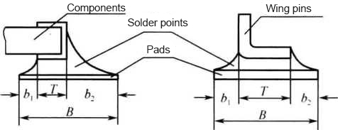
- Calculate pad length based on component lead dimensions and allow for solder fillets.
- Width
- Pad width should exceed lead width by 0.1–0.25 mm for components with spacing over 1.27 mm.
- Symmetry
- Symmetrical pads ensure uniform soldering and prevent displacement.
- Avoiding Issues
- Do not place vias within pads. Maintain at least a 1 mm distance from pad edges.
5. Reference Marks
- Add 1.5 mm copper marks on PCB corners for alignment.
- Include additional marks near fine-pitch ICs (≤0.65 mm) for optical calibration.
6. Other Requirements
- Via Placement
- Avoid vias in pads to prevent solder loss.
- Symbols and Markings
- Ensure markings do not overlap with pads to avoid soldering defects.